Video wird geladen...
Video konnte nicht geladen werden
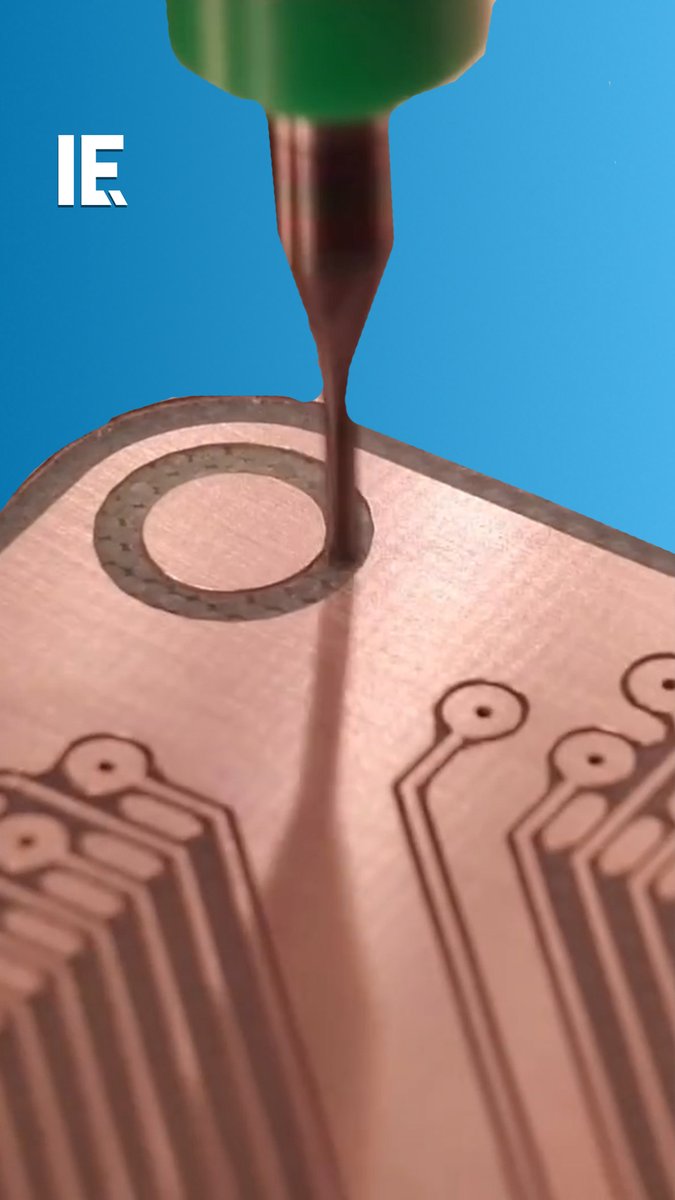
How a printed circuit board is engraved

38,983 Aufrufe • vor 1 Jahr •via X (Twitter)
10 Kommentare

90% of PCBs use photolithography for precision Involves UV light and chemical etching Takes under 30 minutes per board in mass production Copper thickness: 35μm standard Global PCB market: over $90 billion in 2024 Tiny paths, massive impact.

Printed PCB circuit boards can be automatically plugged in more accurately.

Wow. It looks so cool 😎👌

Humans, why waste your time?

@stevewoz thoughts? beautiful right?

The engraving is so precise

Print board

So great!

Well, that head does not double check if the operation was successfull, it just assumes, it works at all times. A better version would check the results in realtime, and would redo if it is not good enough. That would also eliminate quality control checks, at least most of them

This is magic, those a runes.
Ähnliche Videos

![A tool used to install components on a printed circuit board [📹 pcb_liyun1999]](https://image.24vids.com/tw-1931387025942319209/ext_tw_video_thumb/1931386282376306688/pu/img/I5jDh3WumbCx9Abo.jpg)


Best Job Ever, This is how Qur'an Kareem is printed.... MashaAllah!
𝐌𝐚𝐡𝐝𝐢
25,893 Aufrufe • vor 1 Monat