正在加载视频...

视频加载失败

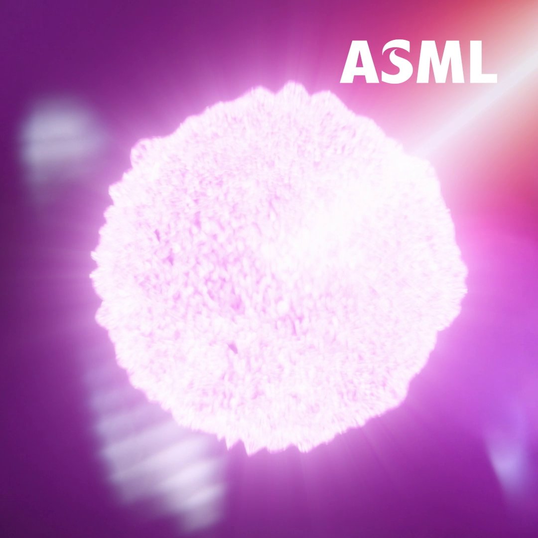
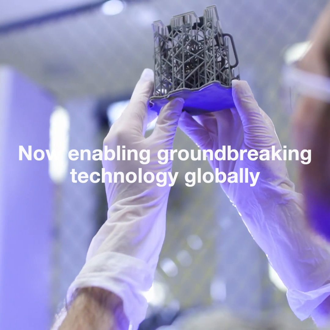
Fly through our High NA EUV system! ⚙️ Discover how our most advanced lithography system harnesses EUV light and anamorphic optics to set new benchmarks for transistor density and chip performance. We are committed to keep powering technology forward with you.

79,998 次观看 • 2 年前 •via X (Twitter)

9 条评论

Luke Zhang 的头像
Luke Zhang2 年前

Can you ship to China?

Trinity 🌸 的头像
Trinity 🌸2 年前

Spice Harvester-developed ,owned & Mfg. by the powerful mining corporation known as CHOAM (Combine Honnete Ober Advancer Mercantiles),they controls most of the economic activity in universe, including prod. & distribution of spice melange( most valuable substance in the universe.

Kenneth 的头像
Kenneth2 年前

It must be said, you people are the Michelangelo of this century when it comes to the art of technology. Keep up the great work that so many millions/billions of people appreciate so much towards tech products.

عبد العزيز الرفاعي 的头像
عبد العزيز الرفاعي1 年前

@mareb_alward

🔴ジョー🇹🇼 的头像
🔴ジョー🇹🇼2 年前

Love this video

Nick 的头像
Nick2 年前

Soar to new heights with our cutting-edge High NA EUV system! 🚀 Discover how our revolutionary technology is pushing the boundaries of chip performance and transistor density using EUV light and anamorphic optics. Let's shape the future of technology together! ⚙️ #Innovation

Senslogic 的头像
Senslogic2 年前

Simply gorgeous.

ALΞXNL.eth 的头像
ALΞXNL.eth2 年前

Awesome video!

Marco De Donno 的头像
Marco De Donno2 年前

why this company is not yet worth 2 trillion $ is still a mystery

相关视频

ACCELERATOR-BASED LITHOGRAPHY AND THE INDUCTION STORAGE RING LIGHT SOURCE The future of chipmaking may look less like a factory and more like a power grid. The proposed “Terafab” paradigm reimagines semiconductor manufacturing at utility scale: chip design, wafer fabrication, EUV lithography, memory, advanced packaging, and testing all under one roof, with the ambition of producing more than one terawatt of AI compute capacity per year. Its most radical innovation is treating light as a utility. Today, each EUV scanner relies on its own laser-produced plasma source, firing lasers at molten tin to generate 13.5 nm light. The process is inefficient, intensely hot, debris-heavy, and difficult to scale. Terafab replaces those individual sources with centralized, accelerator-driven free-electron lasers capable of distributing multi-kilowatt EUV light across an entire network of scanners. The advantages could be transformative: • No tin contamination or destructive plasma debris • Higher efficiency through electron-beam energy recovery • Greater photon flux to suppress stochastic defects at sub-3 nm nodes • Redundant accelerators that keep scanners operating during maintenance • Tunable wavelengths, potentially enabling 6.x nm “Beyond EUV” lithography THAT LAST POINT MATTERS ENORMOUSLY Conventional EUV is locked to the atomic emission of tin. Free-electron lasers are not. Their wavelength can be tuned through the energy of the electron beam creating a possible path beyond today’s 13.5 nm limit. If realized, Terafab would represent more than a larger semiconductor plant. It would transform lithography from a collection of isolated tools into shared industrial infrastructure. The next era of chipmaking may not be defined by a better machine. It may be defined by an entirely new architecture for manufacturing intelligence at civilization scale.

Lacey

12,579 次观看 • 26 天前