
ASML
@ASMLcompany • 61,481 subscribers
Get the latest news about ASML, our holistic lithography products and our people changing the world, one nanometer at a time.
Shorts


Videos
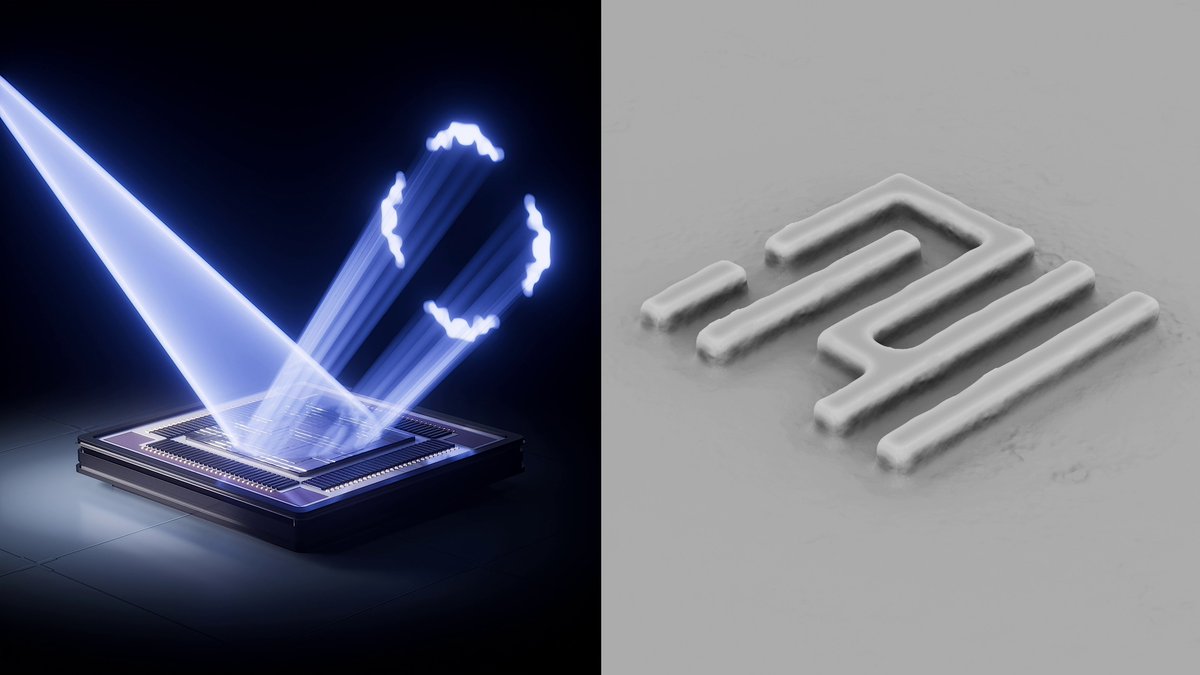
From early design to volume manufacturing, our computational lithography software enables chipmakers to optimize the chip patterning process. Layer by layer, chip by chip, wafer by wafer, computational lithography is helping push microchip technology to new limits.
ASML641,294 görüntüleme • 1 yıl önce
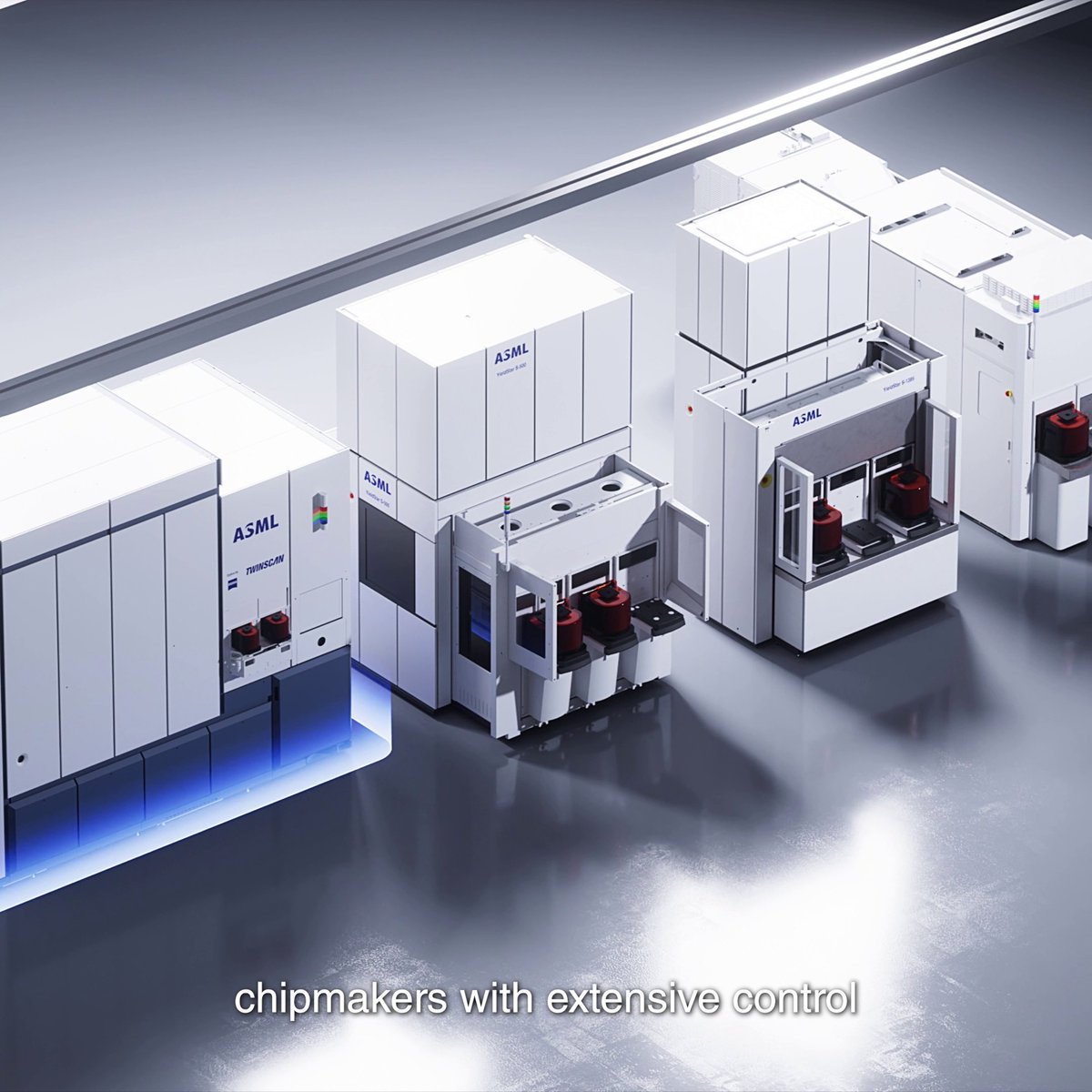
Making advanced chips requires more than advanced lithography. It takes metrology, inspection and computational lithography working together – from R&D to high-volume manufacturing – to keep chipmaking economical. That’s holistic lithography. Watch the animation for more. 👇
ASML73,970 görüntüleme • 3 ay önce

Learning how to precisely print microchip patterns starts in R&D. By integrating computational lithography, optical metrology and e-beam inspection with lithography systems, holistic lithography helps chipmakers fine-tune their patterns before volume production begins.
ASML40,375 görüntüleme • 2 ay önce
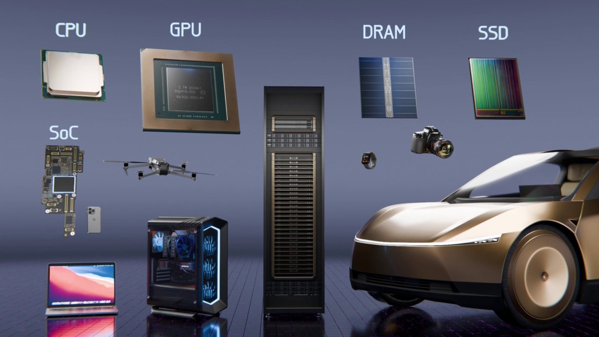
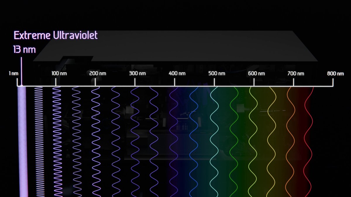
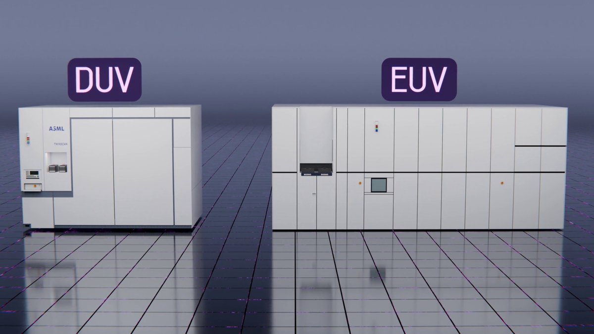
Some microchip layers need extreme ultraviolet (EUV) lithography’s ultra-high resolution, while others can be printed faster with deep ultraviolet (DUV). Chipmakers blend both technologies to optimize for speed, resolution and cost so our devices stay powerful and efficient.
ASML53,009 görüntüleme • 5 ay önce
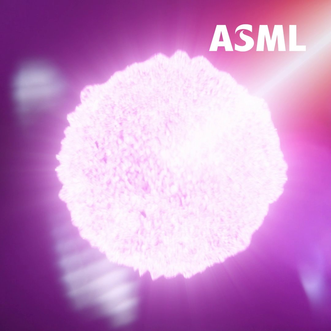
It takes extreme engineering to generate extreme UV light.💥 High NA systems make tin droplets 1/3 the width of a hair and vaporize them to make a plasma 40 times hotter than the sun’s surface. Why? So we keep shrinking chip patterns to keep powering technology forward with you.
ASML75,378 görüntüleme • 10 ay önce


Chips are like tiny skyscrapers that can have more than 100 layers. The lowest, most critical layers form the transistors, while upper layers route power and signals. For chipmakers, choosing the right lithography for each layer is key to balancing precision and cost.
ASML21,264 görüntüleme • 4 ay önce

Daha fazla içerik yok.