正在加载视频...

视频加载失败

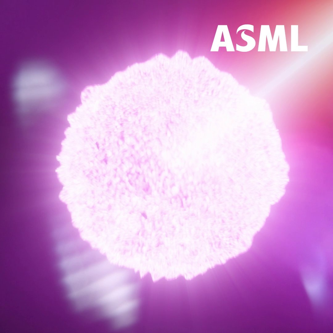
The mind-blowing tech behind microchip manufacturing. Lasers fire 50,000 times per second at tin droplets moving 100 m/s, creating extreme ultraviolet light plasma — and that’s just one step inside ASML’s chip-making machine.

88,207 次观看 • 1 年前 •via X (Twitter)

18 条评论

Science Guy 的头像
Science Guy1 年前

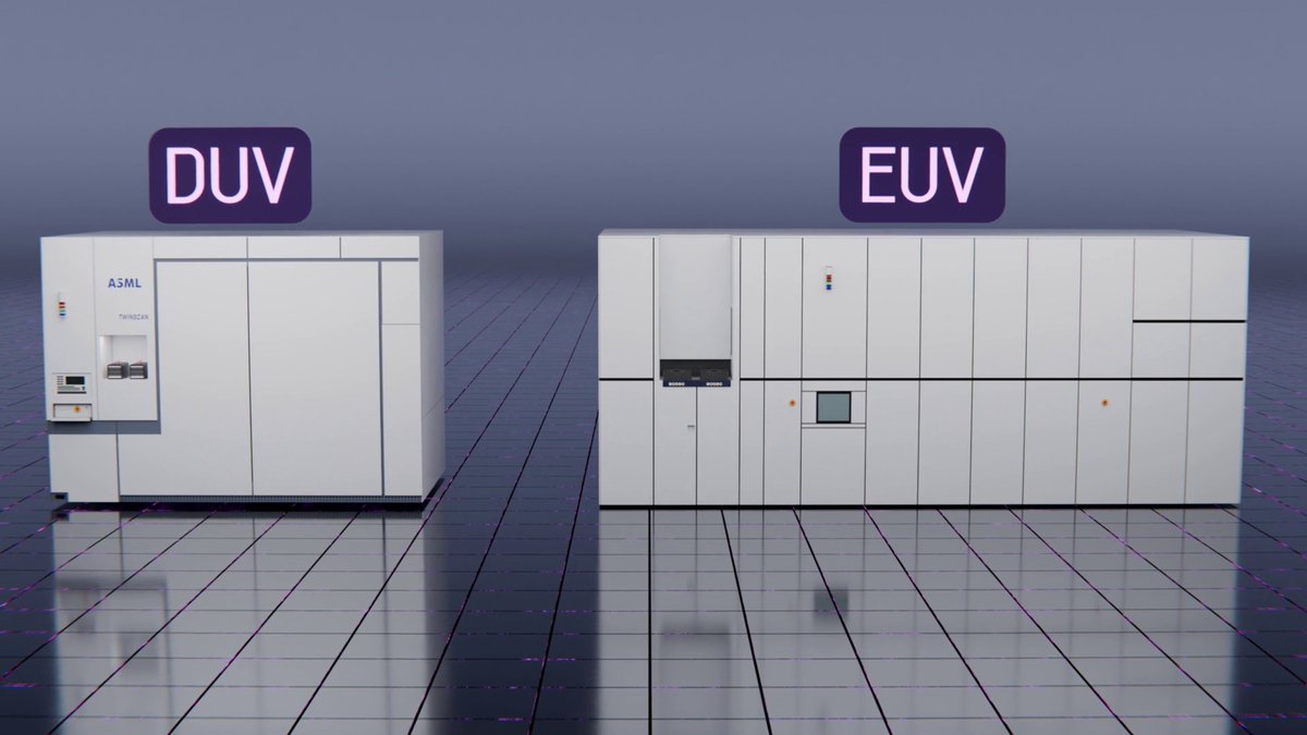
Each ASML extreme ultraviolet (EUV) lithography machine contains over 100,000 individual parts, costs around $400 million, and is the most complex device ever built by humans even more intricate than a space shuttle. The mirrors inside (made by Zeiss in Germany) are so smooth that if they were the size of the United States, the tallest bump would be only 1 millimeter high. And that tin-droplet laser trick? It produces light with a wavelength of 13.5 nanometers so short that ordinary glass would absorb it, meaning the entire system must operate in a vacuum with atomic precision alignment. Every microchip in your phone, computer, or AI server ultimately owes its existence to these laser-fired droplets of molten tin.

RandyT 的头像
RandyT1 年前

Source:

The Gal 的头像
The Gal1 年前

Yep, I used to work for them.

JC 的头像
JC1 年前

I’m convinced this is alien technology. 🤷🏻‍♂️

Loop 的头像
Loop1 年前

ASML’s EUV machines use lasers firing 50,000× per second at tin droplets to create plasma that etches nanometer scale circuits each chip involves billions of precise operations, showing just how extreme semiconductor manufacturing really is

Catalina Castro 的头像
Catalina Castro1 年前

The level of precision here is astounding. Also... a single point of failure.

JETLAB-X 的头像
JETLAB-X1 年前

Wow 😳👍🏽

Kole 的头像
Kole1 年前

Wow

Alberto Yépiz 的头像
Alberto Yépiz1 年前

How they can create 3nm o less with UV light 13nm ? Or there are new lasers from 2nm? @grok

ULTRA 的头像
ULTRA1 年前

What

mewc 的头像
mewc1 年前

Mindblowing

Rajesh M 的头像
Rajesh M1 年前

Truly amazing

Basic 的头像
Basic1 年前

nuts

Fleur Grove 的头像
Fleur Grove1 年前

ASML, c’est du futur en barre ! Si seulement on pouvait lâcher les sudoku administratifs en France et passer aux lasers 😅🤖.

kushyphus 的头像
kushyphus1 年前

@elonmusk from first principles should this be this complicated? @grok

Clausius 的头像
Clausius1 年前

@grok Curious who actually came up with the design of EUV machine?

Cornelis van der Bent 的头像
Cornelis van der Bent1 年前

Watch this great documentary if you want to know how ASML works.

deathmage.x .edge🦭 的头像
deathmage.x .edge🦭1 年前

wild to think this powers AI

相关视频

ACCELERATOR-BASED LITHOGRAPHY AND THE INDUCTION STORAGE RING LIGHT SOURCE The future of chipmaking may look less like a factory and more like a power grid. The proposed “Terafab” paradigm reimagines semiconductor manufacturing at utility scale: chip design, wafer fabrication, EUV lithography, memory, advanced packaging, and testing all under one roof, with the ambition of producing more than one terawatt of AI compute capacity per year. Its most radical innovation is treating light as a utility. Today, each EUV scanner relies on its own laser-produced plasma source, firing lasers at molten tin to generate 13.5 nm light. The process is inefficient, intensely hot, debris-heavy, and difficult to scale. Terafab replaces those individual sources with centralized, accelerator-driven free-electron lasers capable of distributing multi-kilowatt EUV light across an entire network of scanners. The advantages could be transformative: • No tin contamination or destructive plasma debris • Higher efficiency through electron-beam energy recovery • Greater photon flux to suppress stochastic defects at sub-3 nm nodes • Redundant accelerators that keep scanners operating during maintenance • Tunable wavelengths, potentially enabling 6.x nm “Beyond EUV” lithography THAT LAST POINT MATTERS ENORMOUSLY Conventional EUV is locked to the atomic emission of tin. Free-electron lasers are not. Their wavelength can be tuned through the energy of the electron beam creating a possible path beyond today’s 13.5 nm limit. If realized, Terafab would represent more than a larger semiconductor plant. It would transform lithography from a collection of isolated tools into shared industrial infrastructure. The next era of chipmaking may not be defined by a better machine. It may be defined by an entirely new architecture for manufacturing intelligence at civilization scale.

Lacey

13,405 次观看 • 3 个月前