正在加载视频...

视频加载失败

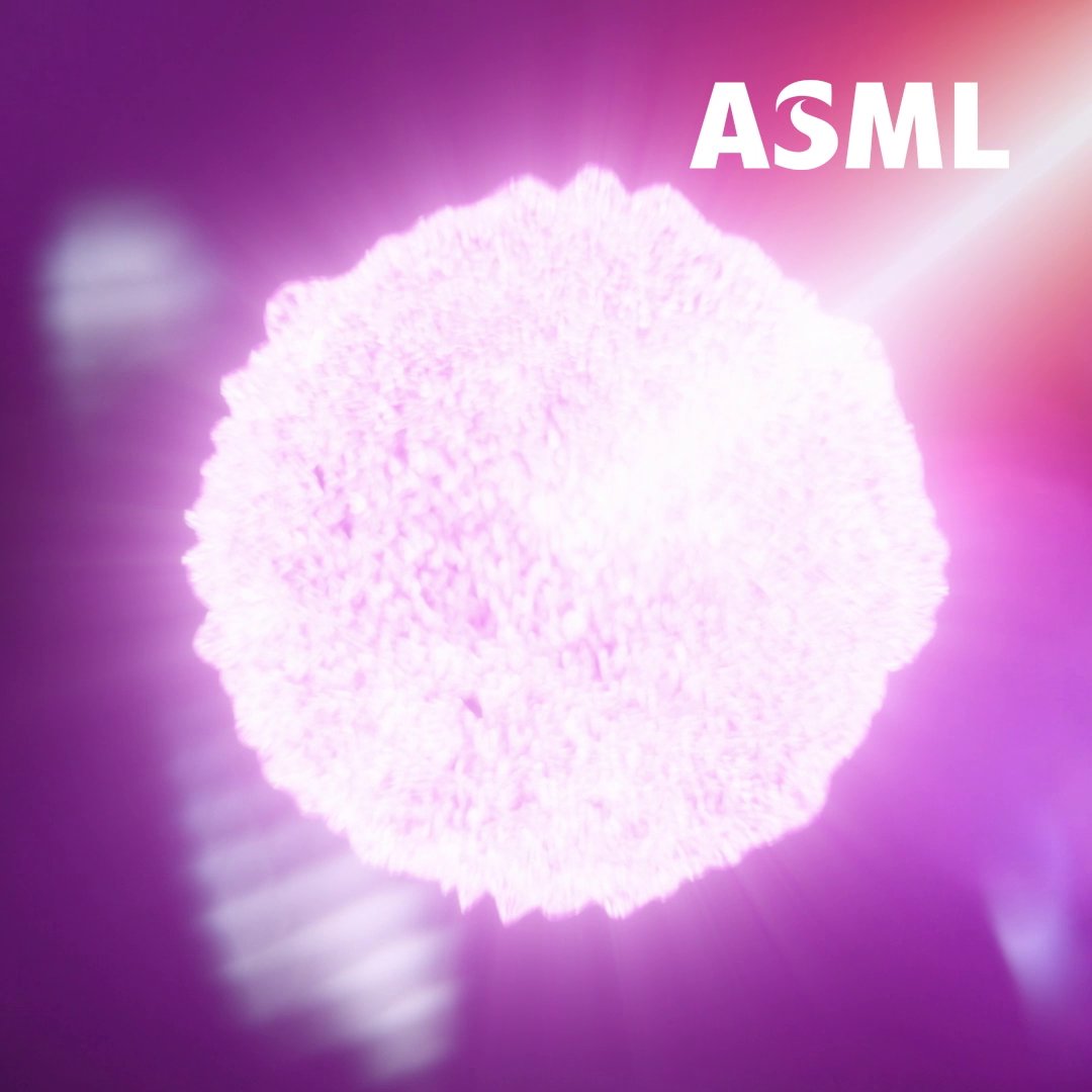
This single $300 MILLION machine fires lasers at tin droplets 50,000 times per second creating plasma hotter than the sun and without it your phone and modern AI wouldn’t exist.

87,065 次观看 • 6 个月前 •via X (Twitter)

0 条评论

暂无评论

原始帖子的评论将显示在这里

相关视频

.Dwarkesh Patel: By 2030, it will be less expensive to monitor every single nook and cranny in America than it is to remodel the White House. “Mass surveillance is, at least in certain forms, already legal. It has just been impractical to enforce so far. Under current law, you have no Fourth Amendment protection against any data you share with a third party. That includes your bank, your ISP, your phone carrier, and your email provider. The government reserves the right to purchase and read this data in bulk without a warrant. What’s been missing is the ability to actually do anything with all of this data — no agency has the manpower to monitor every single camera, read every single message, and cross-reference every single transaction. However, that bottleneck goes away with AI. There are 100 million CCTV cameras in America. You can get pretty good open source multimodal models for 10 cents per million input tokens. So if you process a frame every ten seconds, and each frame is 1,000 tokens, then for 30 billion dollars, you can process every single camera in America. And remember that a given level of AI ability gets 10x cheaper every single year - so a year from now it’ll cost 3 billion, and then a year after 300 million, and by 2030, it’ll be less expensive to monitor every single nook and cranny in this country than it is to remodel the White House. Once the technical capacity for mass surveillance and political suppression exists, the only thing standing between us and an authoritarian state is the political expectation that this is not something we do here.”

Arjun Khemani

145,706 次观看 • 5 个月前

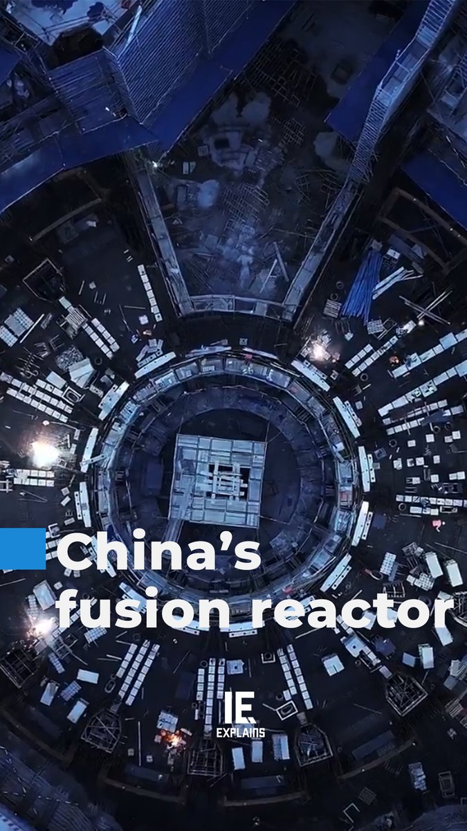
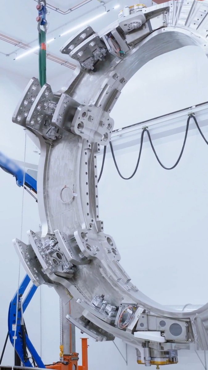
Researchers at Tokamak Energy have captured for the first time a real-time, high-speed video of plasma behaviour inside their ST40 spherical tokamak, tracking visible green and red light emissions as the fusion process occurs. This visual insight comes via a camera operating at thousands of frames per second, offering unprecedented detail of how the plasma evolves, interacts with the surrounding lithium blanket and outer regions, and ultimately radiates energy. The imaging enables scientists to observe how the ultra-hot core transitions outward into cooler zones, how magnetic confinement shapes the plasma behaviour, and how impurities or outer-region interactions influence the process. By giving a ‘star-in-a-donut’ view of fusion in action, this breakthrough adds a new diagnostic tool to the development of fusion energy, helping engineers refine the magnetic confinement, optimise plasma stability and better understand the heat and light flows at play. It was slowed down by 100x. All this was for 0.3s A tokamak is one of the most advanced devices ever created to achieve controlled nuclear fusion, the same process that powers the Sun. Its goal is simple in principle but incredibly challenging in practice: heat a gas until it becomes plasma, raise that plasma to over 100 million degrees, and confine it long enough for hydrogen nuclei to fuse and release energy. Because no material container can survive such temperatures, a tokamak uses powerful magnetic fields to hold and shape the plasma like an invisible cage. The device has a distinctive doughnut-shaped (toroidal) chamber surrounded by magnetic coils. When the machine is switched on, electric currents and external magnets work together to create helical magnetic fields that trap the plasma and keep it away from the walls. As the plasma spirals around these magnetic lines, it heats up dramatically. Additional heating comes from methods like radio-frequency waves and neutral-beam injection, pushing the plasma toward the extreme temperatures needed for fusion. Inside this tightly controlled environment, hydrogen isotopes such as deuterium and tritium can collide and fuse, releasing fast neutrons and a burst of energy. The goal of tokamak research is to reach a point where the fusion reactions produce more energy than the system consumes, a milestone known as “net energy gain.” Modern machines like ITER, JET, and Tokamak Energy’s ST40 are bringing this vision closer, using advanced diagnostics, superconducting magnets, and increasingly stable plasma control. 👉

Erika 

162,540 次观看 • 9 个月前

ACCELERATOR-BASED LITHOGRAPHY AND THE INDUCTION STORAGE RING LIGHT SOURCE The future of chipmaking may look less like a factory and more like a power grid. The proposed “Terafab” paradigm reimagines semiconductor manufacturing at utility scale: chip design, wafer fabrication, EUV lithography, memory, advanced packaging, and testing all under one roof, with the ambition of producing more than one terawatt of AI compute capacity per year. Its most radical innovation is treating light as a utility. Today, each EUV scanner relies on its own laser-produced plasma source, firing lasers at molten tin to generate 13.5 nm light. The process is inefficient, intensely hot, debris-heavy, and difficult to scale. Terafab replaces those individual sources with centralized, accelerator-driven free-electron lasers capable of distributing multi-kilowatt EUV light across an entire network of scanners. The advantages could be transformative: • No tin contamination or destructive plasma debris • Higher efficiency through electron-beam energy recovery • Greater photon flux to suppress stochastic defects at sub-3 nm nodes • Redundant accelerators that keep scanners operating during maintenance • Tunable wavelengths, potentially enabling 6.x nm “Beyond EUV” lithography THAT LAST POINT MATTERS ENORMOUSLY Conventional EUV is locked to the atomic emission of tin. Free-electron lasers are not. Their wavelength can be tuned through the energy of the electron beam creating a possible path beyond today’s 13.5 nm limit. If realized, Terafab would represent more than a larger semiconductor plant. It would transform lithography from a collection of isolated tools into shared industrial infrastructure. The next era of chipmaking may not be defined by a better machine. It may be defined by an entirely new architecture for manufacturing intelligence at civilization scale.

Lacey

12,186 次观看 • 15 天前