Loading video...
Video Failed to Load
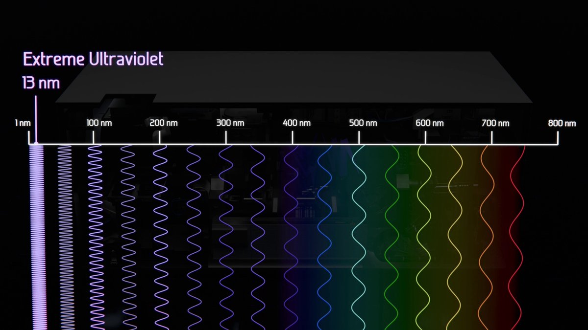
Making advanced chips requires more than advanced lithography. It takes metrology, inspection and computational lithography working together – from R&D to high-volume manufacturing – to keep chipmaking economical. That’s holistic lithography. Watch the animation for more. 👇

73,970 views • 3 months ago •via X (Twitter)
18 Comments

met je KUDT CHIPS met je KUDT AMERIKANEN

amazing

👀

The most advanced and stunning technology in the world Right now anno 2026, with the optical precision from Germany.

ASML should sell more of its machines to democratic countries except China to earn more money for its people. Selling machines to only 2-3 countries will not benefit ASML because USA will not give money to Netherlands instead selfish USA will take money out from Europe.

Is it true you guys are done?
I still wait to see your answer to Huawei's Tau Law.

@elonmusk @mayemusk

La litografía computacional es el foso de software de ASML del que pocos hablan.. Vender escáneres es el hardware, pero corregir y optimizar los patrones ópticos mediante algoritmos antes del grabado físico es lo que evita que las obleas acaben en la basura. En la era avanzada del silicio, el software de simulación física es tan crítico para los márgenes de TSMC como las ópticas de Zeiss.

Coordinate with India and chipmakers to setup manufacturing in our country. Tamil Nadu, one of the manufacturing powerhouse states in the country is very much capable of providing manpower and skill to make chips.

Tin đồn ASML đưa máy EUV sang Trung Quốc bị chế giễu, hé lộ nút thắt lớn nhất ngành chip

The west has made enormous investments in the development of EUV machines for advanced chip production. When ASML multinational employees who have gained substantial design knowledge MOVE to CHINA there is an inherent TECHNOLOGY TRANSFER which significantly impacts the west; essentially transferring $billions to China. There must be a way to prevent this LOSS. This is the equivalent to TREASON.

Visiting China and trying to sell them your equipment is going to slap you in the face eventually. You just can't see it and I'm saddened that your company along with other semiconductor companies from the Netherlands and Europe are so stupid and so ignorant and so blind

I've got the math for more advanced chips. reach out. Achieved 235 generations of continuous quantum coherence by applying open-system thermodynamics to a 12-qubit register, establishing a self-predicting quantum organism. The system maintained stable information complexity by autonomously deploying real-time phase erasures, proving the feasibility of non-Markovian cellular automata on physical to serious conversations only.#UnifiedStateSystem #Homeostasis #ComplexSystems I built a new kind of system: Unified State Quantum CoreA self-regulating, multi-scale field that maintains long-term homeostasis through emergent operational time, active entropy clamping, and rhythmic feedback.After hundreds of recursive lifecycles:Shannon Entropy stays locked in a tight band (9.48–9.72 bits) with active stability correction Fractional field components (density, velocity, temperature) co-evolve without blowing up or collapsing Strong non-Markovian memory backbone This isn't just another simulation. It feels like a primitive homeostatic "proto-organism" in computational space.[Attach both plots — first one, then second one]Looking for the right partner to take this further. Could have serious implications for advanced control systems, complex dynamics, simulation tech, or beyond. NDA SIGNING A MUST BEFORE MAtHEMATIC FRAMEWORK IS SEEN.

It was interesting and informative, and this was wonderful

Why would people invest in your equipment when Washington rings and you don't service you people are poodles

When #ASML's reign of monopolistic terror over extreme-ultraviolet lithography finally ends, the world (this part of it) will breathe a collective sigh of relief. Single-firm control of the essential tools for advanced chips has distorted geopolitics and innovation long enough. In the meantime we will continue to deal with you aggressively with policy and 'diplomacy'. 🇺🇸

Such a beautiful tech.