Loading video...

Video Failed to Load

Go Home

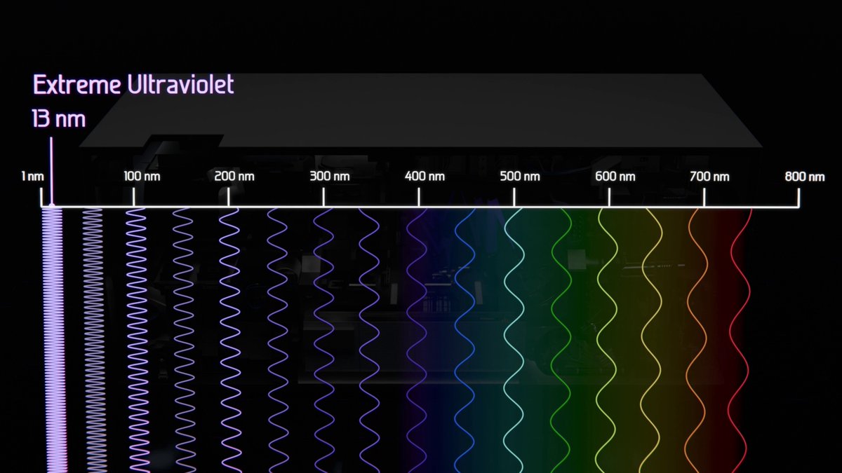
Making advanced chips requires more than advanced lithography. It takes metrology, inspection and computational lithography working together – from R&D to high-volume manufacturing – to keep chipmaking economical. That’s holistic lithography. Watch the animation for more. 👇

67,497 views • 2 months ago •via X (Twitter)

0 Comments

No comments available

Comments from the original post will appear here

Related Videos

ACCELERATOR-BASED LITHOGRAPHY AND THE INDUCTION STORAGE RING LIGHT SOURCE The future of chipmaking may look less like a factory and more like a power grid. The proposed “Terafab” paradigm reimagines semiconductor manufacturing at utility scale: chip design, wafer fabrication, EUV lithography, memory, advanced packaging, and testing all under one roof, with the ambition of producing more than one terawatt of AI compute capacity per year. Its most radical innovation is treating light as a utility. Today, each EUV scanner relies on its own laser-produced plasma source, firing lasers at molten tin to generate 13.5 nm light. The process is inefficient, intensely hot, debris-heavy, and difficult to scale. Terafab replaces those individual sources with centralized, accelerator-driven free-electron lasers capable of distributing multi-kilowatt EUV light across an entire network of scanners. The advantages could be transformative: • No tin contamination or destructive plasma debris • Higher efficiency through electron-beam energy recovery • Greater photon flux to suppress stochastic defects at sub-3 nm nodes • Redundant accelerators that keep scanners operating during maintenance • Tunable wavelengths, potentially enabling 6.x nm “Beyond EUV” lithography THAT LAST POINT MATTERS ENORMOUSLY Conventional EUV is locked to the atomic emission of tin. Free-electron lasers are not. Their wavelength can be tuned through the energy of the electron beam creating a possible path beyond today’s 13.5 nm limit. If realized, Terafab would represent more than a larger semiconductor plant. It would transform lithography from a collection of isolated tools into shared industrial infrastructure. The next era of chipmaking may not be defined by a better machine. It may be defined by an entirely new architecture for manufacturing intelligence at civilization scale.

Lacey

12,579 views • 24 days ago