Loading video...
Video Failed to Load
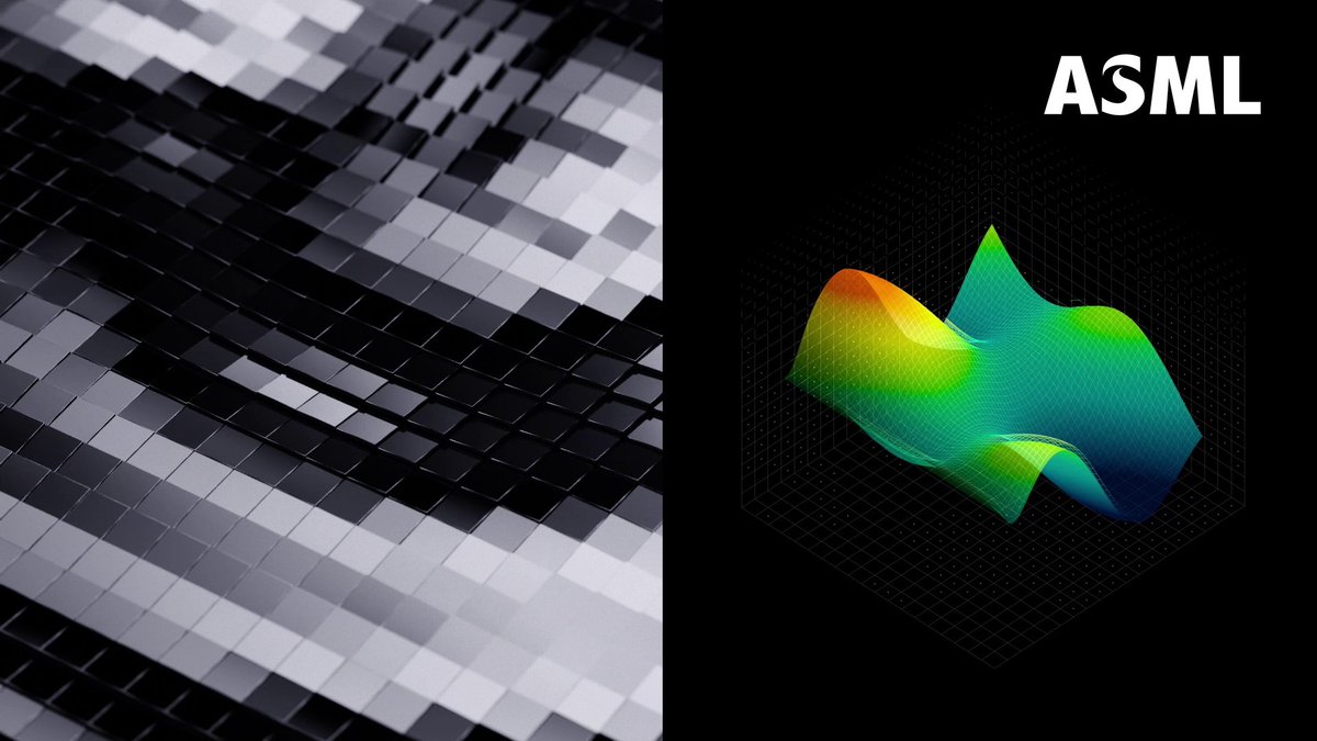
Transferring chip patterns from masks to wafers can cause deformations. That’s why we correct for optical effects with mask optimization: a computational lithography process that adds features to chip blueprints to correct patterns so they appear exactly as intended on the wafer.

11,698 views • 9 months ago •via X (Twitter)
0 Comments
No comments available
Comments from the original post will appear here





![here are the jp subs for this scene 😵💫: 🐿️something you see at home that you can ride 🐰han jisung! 🦊so true! 💬[that’s exactly right] 🦊correct! next card! 🐰han jisung! 💬[bewildered gatekeeper] 🐿️correct! next card! 🐺I’ll take that answer 💬[too perfect an answer to get even one “no”] 🦊I approve 💬[can prove it’s true right now] 🐰I can show you right here 💬[I politely decline, your majesty] 🐿️no, thank you](https://image.24vids.com/tw-1975616738705482077/amplify_video_thumb/1975616670430527488/img/2qCFIyxXlRPW0vIU.jpg)